Worldwide Laser Service Corp. Awarded Contract for Three [3] Wafer Marking Systems
Worldwide Laser Service Corporation is pleased to announce we have been awarded a contract for three [3] new wafer marking systems by a major N. American manufacturer

GILBERT, Ariz., Sept. 13, 2018 /PRNewswire-PRWeb/ -- Worldwide Laser Service Corp. (WLSC) has been awarded a contracts to build three [3] new laser wafer marking systems by a major N. American manufacturer.
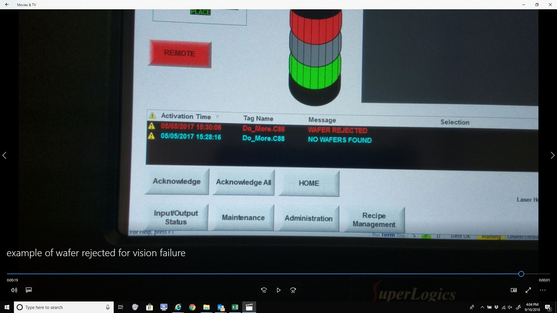
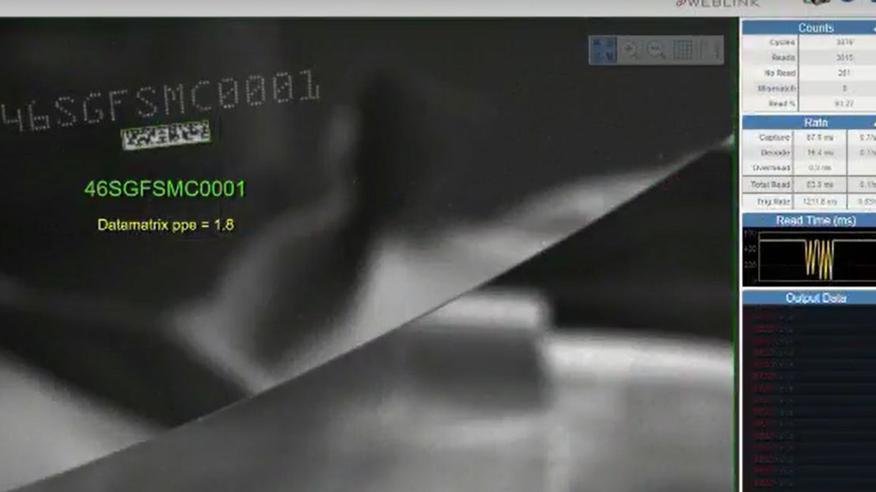
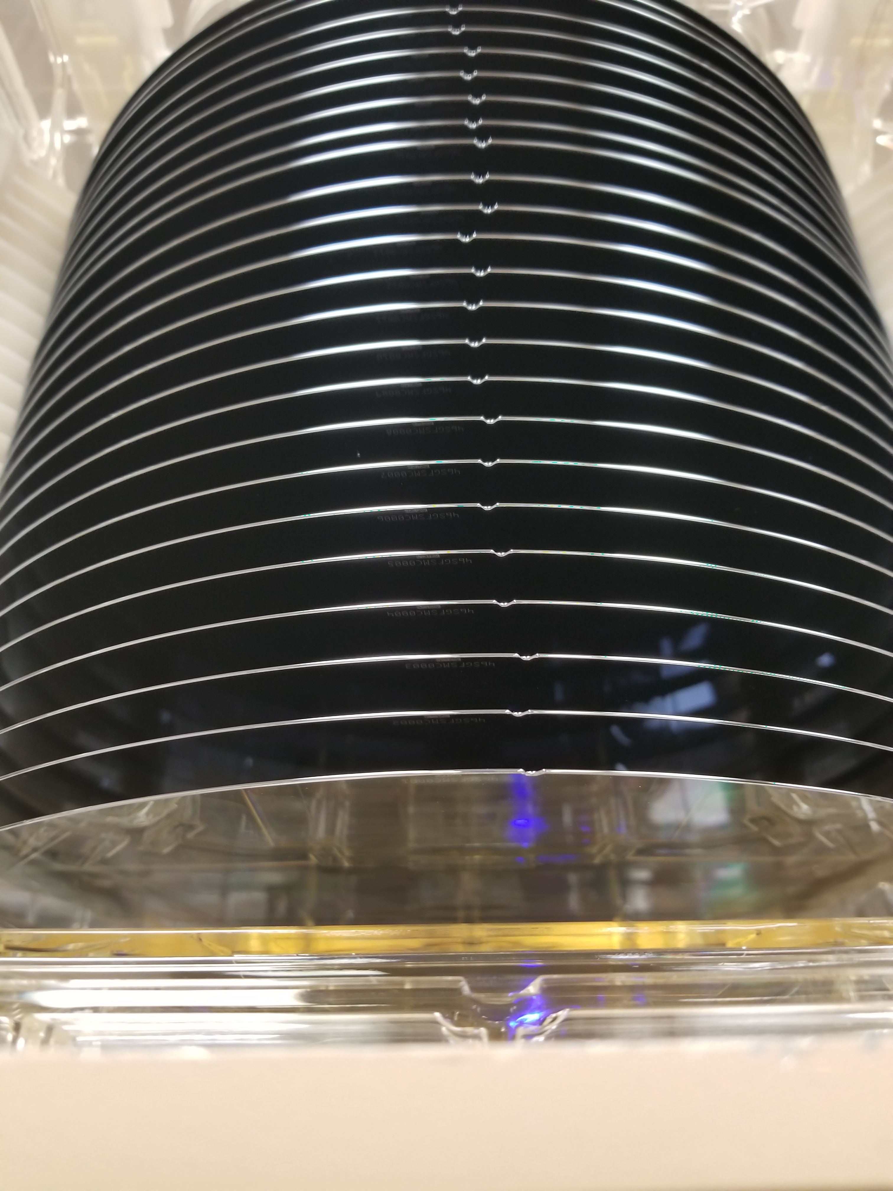
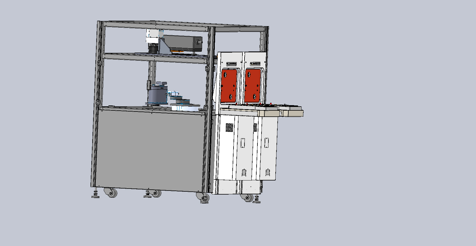
The wafer marking systems will be designed to handle wafers up to 300mm size and fully integrated into the customers production systems for remote [no operator] control. The Systems will be fully compliant with GEMSECS standards. Wafer marking systems from WLSC come in several different standard models, manual load and unload of wafers, automated load and unload of wafers with operator intervention for loading and unloading cassettes, and lights out manufacturing allowing for robotic loading of cassettes and complete host control of the system. WLSC wafer marking systems write to individual die with characters as small as 20 micro-meters, generally the smallest die achievable are approximately .6 to .7 mm and if we assume, 1 mm x 1 mm die 70,000 individual die with characters should be achieved on a 300mm wafer. If, however, much larger die were required, say 20mm x 20mm, a yield of approximately 148 individual die would be expected. Cost reduction and increased capacity requirements are driving ever smaller die, however, the point is WLSC systems are configured to be flexible and accommodate many different die requirement allow with host interface and data base reporting requirements. Contact the laser system engineers at WLSC to discuss all aspect of your silicon wafer and semi-conductor laser marking, laser etching, and laser cutting requirements.
Share this article